 Products Home
小型差分ディテクタ
- Differential Photodiode Pair with DC-Coupled Output
- High Quantum Efficiency Models for Quantum Applications
- Low-Artifact Models for OCT Applications
- Volume Pricing Available for OEMs
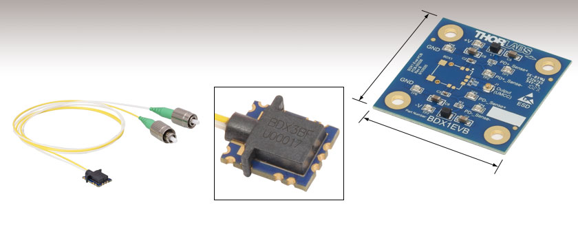
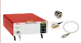
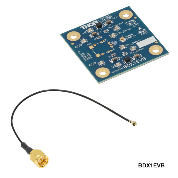
BDX1EVB
Evaluation Board for BDX Family Detectors
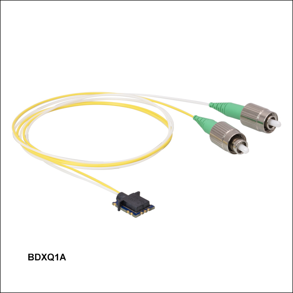
BDXQ1A
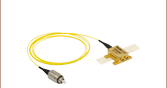
High Quantum Efficiency Compact Balanced Detector with SMF-28e Fiber Leads and FC/APC Connectors
Detail View of a BDX3BF Detector
2.00"
(50.8 mm)
2.00"
(50.8 mm)


Please Wait
| Key Specificationsa,b | ||
|---|---|---|
| Item # Prefix | BDXQ1 | BDX3 |
| Responsivity | 1.2 A/Wc | 0.6 - 0.9 A/Wd |
| -3 dB Bandwidth | DC to 3 GHz | DC to 5 GHz |
| Impulse Response (FWHM) | 120 ps | 70 ps |
| Wavelength Range | 1525 - 1575 nm | 980 - 1625 nm |
- Quantum Detection Systems
- OEM Balanced Detection
- OCT Systems
- LIDAR Systems
- Optical Frequency Domain Reflectometry
- Compact Detection Systems
| Balanced Detector Selection Guide |
|---|
| Balanced Detectors with Fast Monitor Output |
| Large-Area Balanced Amplified Detectors |
| Suitable for OCT |
| Compact Balanced Amplified Detectors |
| Compact Balanced Detectors |
| OCT Balanced Detectors with Fast Monitor Output |
| Auto-Balanced Detector with Avalanche Photodiodes |
| Polarization-Dependent Balanced Detector |

Janis Valdmanis, Ph.D. Optics
Ultrafast Optoelectronics
General Manager
Got Questions?
Our engineers and expertise are here for you!
If you are not sure whether our catalog items meet your needs, we invite you to contact us. Or ask about a loan, so you can try them out for yourself, in your own lab. We can also support custom or OEM requirements you may have.
Just press the button, and we'll get back to you within the next business day.

Features
- High Quantum Efficiency Balanced Differential Photodetectors (Item # Prefix BDXQ1)
- Low-Loss Optical Design to Maximize Efficiency
- Balanced Differential Photodetectors (Item # Prefix BDX3)
- Low-Artifact Performance Optimized for OCT Applications
- Compact Package: 13.0 mm x 11.2 mm x 3.3 mm
- Surface Mount Component (Solders Directly to PCB)
- FC/APC, FC/PC, or LC/PC Connectors
Thorlabs' BDX family of high-speed, compact, fiber optic balanced detectors are designed for demanding OEM applications that require low-artifact performance. The surface mount package contains fiber and photodiode arrays configured on a common substrate for excellent response matching and precise timing for differential signal detection. This design achieves a high common mode rejection ratio (CMRR) and low crosstalk.
The optoelectrical configuration of these detectors is simple and compact in order to support high volume applications where space and cost are a primary concern. Additionally, the compact mounting geometry allows for easy integration with conventional circuit boards and enables high-speed connection to subsequent amplifiers or other components. Our BDX family of detectors do not have built-in amplifiers.
The pair of input fibers direct light to an array of two matched photodiodes biased with positive and negative voltages and wired as a differential pair with a single, common output. This internal optical geometry is designed to eliminate unwanted reflections from traveling either forward or backward along the intended optical path.
The BDXQ1 series of high quantum efficiency compact balanced detectors offer a typical quantum efficiency of 97% at 1550 nm with a frequency response of DC to 3 GHz. They are coupled with a pair of SMF-28e single mode input fibers with Ø900 µm loose-buffer jackets. The pair of fibers on each detector are matched in length to 1 mm and are available from stock with narrow key FC/APC or FC/PC connectors, or with LC/PC connectors upon request.
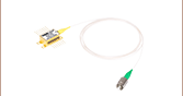
The BDX3 series of compact balanced detectors provide a frequency response bandwidth of DC to 5 GHz and are available with two single mode input fiber options. The BDX3Cx detectors have HI1060 fiber leads with Ø900 µm loose-buffer jackets for applications in the 980 - 1260 nm wavelength range, while the BDX3Bx detectors have SMF-28 Ultra fiber leads with Ø900 µm loose-buffer jackets for single mode applications in the 1260 - 1625 nm wavelength range. The two fibers in each model are matched in length to 1 mm and are available from stock with narrow key FC/APC or FC/PC connectors, or with LC/PC connectors upon request.
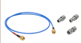
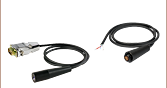
We also offer the BDX1EVB Evaluation Board for testing BDX balanced detectors in a lab environment with common cable connections. This board features a pre-defined footprint for soldering a BDX detector in place, and has specified points for connecting power and current monitor leads. Included with each BDX1EVB evaluation board is a micro-coaxial cable that transmits the high-speed output signal through an SMA connector.
Previous-Generation BDX1x Balanced Detectors
If your application does not require the lower-artifact performance of the BDX3 series detectors, the previous-generation BDX1x balanced detectors that share the same form factor and bandwidth are available upon request by contacting Tech Sales.
Click to Enlarge
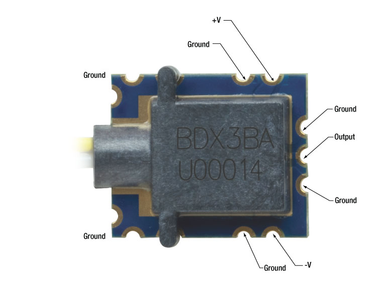
External Pin Connections for the BDX Family of Detectors.

Click to Enlarge
Internal Electrical Configuration for the BDX Family of Detectors.
Operation of the BDX Family of Balanced Detectors
Thorlabs' BDX familly of Balanced Detectors provide differential detection of complementary signals. Each device consists of a fiber array that directs the two optical input signals to an array of well-matched photodiodes (see diagram to the near right). The output is the difference of the two input signals, which results in greatly reduced common mode noise.
The diagram to the far right indicates the external pin connections for each half-via contact of a detector. Soldering of the half-vias must be done cleanly and quickly. To avoid damaging the internal opto-electronic components, do not exceed 5 seconds of soldering time at 250 °C for each contact. When mounting to the BDX1EVB Evaluation Board or other PCB, ensure that all seven half-via contacts near the output are soldered and at least one of the ground contacts in each of the rear corners are soldered for a total of 9 contact points. All soldering must be done by hand; a reflow oven will damage the device. Please refer to the BDX1EVB Evaluation Board spec sheet for complete mounting instructions.
The components inside this module are ESD sensitive. Take all appropriate precautions to discharge personnel and equipment before making any electrical connections to the unit. This also applies to coaxial cables that easily accumulate capacitive change.

Click to Enlarge
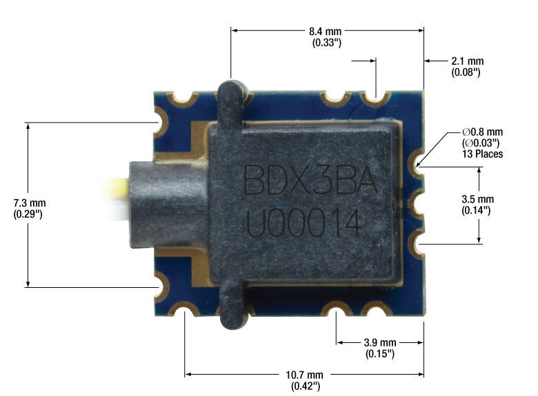
The dimensions in this bottom view of the BDX3BA Balanced Detector are representative of all BDX Detectors.
Click to Enlarge
The dimensions in this top view of the BDX3BA Balanced Detector are representative of all BDX Detectors.
This tab describes how to solder a BDX detector to a BDX1EVB evaluation board or custom PCB. This procedure is recommended for users who are experienced with soldering. For additional details regarding the operation of the BDX1EVB board, please refer to the BDX1EVB board spec sheet.
Materials and Equipment
- Epoxy Gel, Quick-Curing at 75 °C
- Solder Appropriate for Soldering Components to PCBs
- Flux Designed to Work with the Chosen Solder
- Hot Plate Capable of Maintaining a Temperature of 75 °C
- Soldering Iron with Tip Capable of Fitting Inside BDX Detector Edge Castellations
Recommended Soldering Procedure
The steps below are the recommended procedure for soldering a BDX detector to a BDX1EVB evaluation board. Steps 5-6 are shown for two contacts in the video to the right.
Note: Soldering must be done cleanly and quickly. For each contact, do not exceed 5 seconds of soldering time at 250 °C contact temperature, to avoid damaging the internal opto-electronic components.
1. With the BDX1EVB board on the hot plate (heating off), place a small bead of epoxy gel in the center of the BDX footprint. Only a small amount of epoxy should be used to ensure that it does not leak out onto the soldering contacts. To ensure that unwanted movement does not occur, the board can be taped to the hot plate using a tape rated for 75 °C.
2. Place the BDX detector onto the footprint on the evaluation board, ensuring that the alignment pins go through the holes in the board. Ensure that the edge castellations are aligned with the pads on the board as closely as possible.
3. Turn the hot plate to 75 °C and leave for long enough to let the epoxy cure.
4. With the hot plate still at 75 °C, set the temperature of the soldering iron to 400 °C.
5. Using a small syringe, apply a small amount of flux to each pad and adjacent castellation on the detector, ensuring that both are coated, as shown in the video above.
6. Working quickly, apply a small amount of solder to the iron tip, then touch the tip to the castellation and pad simultaneously. If needed, add extra solder. A clean, shiny fillet should form between the pad and the castellation. If forming a fillet is difficult, using a lower-temperature solder may help.
7. Repeat steps 5-6 for each of the seven contacts near the output and the bias, as well as at least one of the ground contacts in each of the rear corners.
8. Clean the excess flux with a polyester cleanroom swab dipped in isopropyl alcohol.
| Posted Comments: | |
William Rosas
(posted 2024-06-14 10:41:53.877) Hello.
Thanks for such interesting products. Could you please provide a value for the NEP of your fast detectors?
Best regards,
William cdolbashian
(posted 2024-06-28 12:00:11.0) Thank you for reaching out to us with this inquiry. The NEP of a device is derived largely from the Thermal and Shot noise within a given device. Depending on the configuration of your electronics, these values will change, and as a result the NEP will vary. I have contacted you directly to assist in estimation of the NEP for your given system implementation. Taylor Bates
(posted 2024-01-12 13:40:29.01) Are any plans in the future for you all to have a Silicon version of these detectors for fast balanced detection at shorter wavelengths? Thanks in advance. ksosnowski
(posted 2024-01-17 04:12:54.0) Hello Taylor, thanks for reaching out to Thorlabs. We are currently developing BDX modules for visible wavelengths, but they will use a GaAs photodiode array rather than Silicon. We do not however have an expected timeline for this new product currently. Glenn Goranson
(posted 2022-01-27 11:57:12.16) Is there an option for a 2050nm version of this device? What is the noise level? What would it take for a custom solution? Thanks. cdolbashian
(posted 2022-02-10 11:43:18.0) Thank you for reaching out to us with this inquiry! If you are referring to the dark noise of this device, we spec <50nA of dark current, though the typical value is <10nA under a 10V bias. Regarding a custom solution, I have reached out to you directly to discuss your specific requirements. In the future, please feel free to contact techsales@thorlabs.com for your custom inquiries! Minji Hyun
(posted 2022-01-04 07:02:22.28) Is there any information on series resistance of BDX1BA? cdolbashian
(posted 2022-01-04 11:52:04.0) Thank you for reaching out to us here at Thorlabs. The series resistance of the BDX1BA device is typically on the order of a few Ohms. |

 ズーム
ズーム- 97% Quantum Efficiency at 1550 nm
- Low-Loss Optical Design to Maximize Efficiency
The BDXQ1 series high quantum efficiency balanced differential photodetectors are designed to maximize quantum efficiency at 1550 nm to preserve every photon. These detectors offer a responsivity of 1.2 A/W at 1550 nm with a bandwidth of 3 GHz. They require a ±12 V bias voltage and are coupled with a pair of SMF-28e single mode input fibers with Ø900 µm loose-buffer jackets. The pair of fibers on each detector are matched in length to 1 mm and are available from stock with narrow key FC/APC or FC/PC connectors, or with LC/PC connectors upon request.
| Key Specsa,b | |||||||||
|---|---|---|---|---|---|---|---|---|---|
| Item # | Full Specs |
-3 dB Bandwidth |
Impulse Response |
Wavelength Range |
Responsivity | Quantum Efficiency | Fiber Connector | Fiber Type | Mode Field Diameter |
| BDXQ1A | DC - 3 GHz | 120 ps | 1525 - 1575 nm | 1.2 A/W @ 1550 nm | 97% @ 1550 nm | FC/APCc | SMF-28e | 10.4 ± 0.5 µm @ 1550 nm | |
| BDXQ1F | FC/PCc | ||||||||
- For complete specifications, please click the blue info icons (
 ) next to each Item #.
 - All specifications are typical values at 25 °C. Best performance is obtained when input powers are balanced. Fiber connecter alignment can introduce imbalance in the input powers.
- 2.0 mm Narrow Key

 ズーム
ズーム- Low Internal Reflection Design to Minimize Artifacts for OCT Applications
- Available in 980 - 1260 nm or 1260 - 1625 nm Wavelength Ranges
The BDX3 series compact balanced detectors provide a frequency response bandwidth of DC to 5 GHz and are optimized for low-artifact performance, ideal for OCT applications. These detectors require a ±5 V bias voltage and are available with two single mode input fiber options. The BDX3Cx detectors have HI1060 fiber leads with Ø900 µm loose-buffer jackets for applications in the 980 - 1260 nm wavelength range, while the BDX3Bx detectors have SMF-28 Ultra fiber leads with Ø900 µm loose-buffer jackets for single mode applications in the 1260 - 1625 nm wavelength range. The two fibers in each model are matched in length to 1 mm and are available from stock with narrow key FC/APC or FC/PC connectors, or with LC/PC connectors upon request.
| Key Specsa,b | ||||||||
|---|---|---|---|---|---|---|---|---|
| Item # | Full Specs |
-3 dB Bandwidth |
Impulse Response |
Wavelength Range |
Responsivity | Fiber Connector | Fiber Type | Mode Field Diameter |
| BDX3CA | DC - 5 GHz | 70 ps | 980 - 1260 nm | 0.6 A/W @ 1060 nm | FC/APCc | HI1060 | 6.2 ± 0.3 µm @ 1060 nm | |
| BDX3CF | FC/PCc | |||||||
| BDX3CL | LC/PC | |||||||
| BDX3BA | 1260 - 1625 nm | 0.8 A/W @ 1310 nm 0.9 A/W @ 1550 nm |
FC/APCc | SMF-28 Ultra | 9.2 ± 0.4 µm @ 1310 nm 10.4 ± 0.5 µm @ 1550 nm |
|||
| BDX3BF | FC/PCc | |||||||
| BDX3BL | LC/PC | |||||||
- For complete specifications, please click the blue info icons () next to each Item #.
- All specifications are typical values at 25 °C. Best performance is obtained when input powers are balanced. Fiber connecter alignment can introduce imbalance in the input powers.
- 2.0 mm Narrow Key

 ズーム
ズーム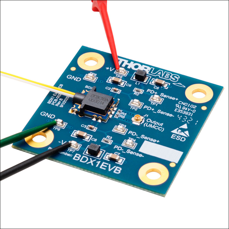
Click to Enlarge
差分ディテクタBDX3BAを評価ボードBDX1EVBにはんだ付けし、正/負のリード線とアース線をはんだで接続した様子
- BDXシリーズディテクタを取り付けるためのプリント回路基板(PCB)
- PD電流モニタ用のテストポイント
- UMCC-to-SMA同軸出力ケーブル
評価ボードBDX1EVBを使用することで、BDXシリーズディテクタを所定の位置にはんだ付けで取り付けられるため、一般的なケーブルとコネクタを使用して電源と出力部を接続することができます。BDXシリーズディテクタ周囲のハーフビアコンタクトは、あらかじめ設定された評価ボードの接触点にはんだ付けできます。評価ボードBDX1EVBには、高速の出力信号をSMAコネクタを通じて伝送するためのマイクロ同軸ケーブルが付属します。
当社の評価ボードBDX1EVBには、アースおよび電源接続用の接続点がラベル表示されています。4つのテストポイントは各PDの光電流をモニタするために使用できます。フォトダイオードの正入力(PD+)をモニタリングするには、テストポイントTP1とTP2を使用して、電流検出抵抗器R2の両端に高インピーダンス電圧計を接続します。同様に、フォトダイオードの負入力(PD-)をモニタリングするには、テストポイントTP3とP4を使用して、電流検出抵抗器R2の両端に高インピーダンス電圧計を接続します。この電圧計は光電流1 mAごとに10 mVを読み取ります。電源、アース、テストポイントの接続には、スプリングフックを使用した標準的なテストリード(別売りです)をご使用ください。評価ボードBDX1EVBの接続および動作についての詳細は、BDX1EVBのスペックシートをご覧ください。
モジュール内の部品は静電気により容易に破壊されます。電気的な接続を行う前に、必ず取扱者や機器に対して適切な放電防止対策を講じてください。この対策は、同軸ケーブルの取り扱いの際にも当てはまります。 はんだ付けはすべて手動で行ってください。リフロー炉の使用はデバイスの損傷につながります。詳しい取付方法については、評価ボードBDX1EVBのスペックシートをご覧ください。推奨するはんだ付けの手順については「はんだ付け」のタブでご紹介しています。