 Products Home
半導体光増幅器、Oバンド(1285~1350 nm)、偏光依存型(BOA)
- Polarization-Dependent Booster Optical Amplifiers
- SM or PM Fiber-Pigtailed Butterfly Package
- High Saturation Power (>15 dBm)
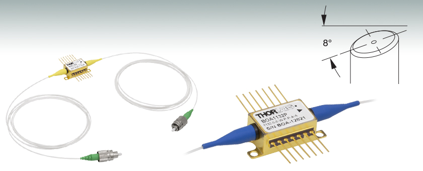
BOA1130S
High-Power BOA with SM Fiber and FC/APC Connectors
BOA1132P
BOA with PM Fiber and FC/APC Connectors, Closeup of Butterfly Package Shown
FC/APC Connectors


Please Wait
| Optical Amplifier Selection Guide |
|---|
| 780 - 795 nm BOAs |
| 830 nm BOAs |
| 930 nm BOAs |
| 980 nm BOAs |
| 1050 nm BOAs |
| 1210 nm BOAs |
| 1250 nm BOAs |
| O-Band (1285 - 1350 nm) BOAs |
| E-Band (1410 nm) BOAs |
| C-Band (1550 nm) BOAs and SOAs |
| L-Band (1590 - 1625 nm) BOAs |
| 1685 nm BOAs |

Click to Enlarge
電流がリッジ導波路に印加されると、励起状態の電子が入射光の刺激を受けます。これにより光子が複製され、信号利得が得られます。
特長
- 偏波保持:1つの偏光状態のみを増幅
- 1285 nm~1350 nmの間の中心波長をご用意
- 1.5 m長のシングルモードまたは偏波保持ファイバーピグテール
- 2.0 mmのナローキー付きFC/APCコネクタ
- チップの両端で2.5 dBの結合損失
- 高い飽和出力(>15 dBm)、高効率
- 3 dB帯域幅: 70 nm、80 nm、82 nm、87 nm (典型値)
- 両端面にARコーティング加工(R<0.1%)
- 一般的な用途:変調、トランスミットMUX/DeMUXの挿入損失の補償、光シャッタ
半導体光増幅器は、シングルパスの進行波増幅器で、単色信号あるいは多波長信号の両方において性能を発揮します。偏光依存型半導体光増幅器(BOA)は1つの偏光状態のみを増幅するので、入力光の偏光状態が分かっている条件での使用に適しています。これに対して入力信号の偏光状態が不明の場合や変動する用途では、偏光無依存型半導体光増幅器(SOA)が必要となります。しかしながら利得、雑音、バンド幅や飽和出力強度の仕様は、偏光依存型(BOA)の方が偏光無依存型(SOA)と比較して優れています。これは偏光無依存型(SOA)では偏光無依存の特性を付与している設計により上記特性が犠牲になっているためです。
偏光依存型半導体光増幅器(BOA)は、高効率のInP/InGaAsP多重量子井戸(MQW)構造です。右の概略図でもご覧いただけるよう に、増幅器の入出力光は、光増幅器のチップ上の信頼性の高いリッジ導波路に結合されています。損失の典型値はファイバからチップ、そしてチップからファイバの両方の結合において1.5~2.5 dBです。この結合損失は、総利得、雑音指数(NF)、飽和出力強度(Psat)に影響を及ぼします。増幅によって得られる利得が損失を上回ったとしても、これらの損失はデバイスの性能に重要な影響を与えます。例えば、入力結合効率が1 dB減少した場合、雑音指数は1 dB増加します。これに対して出力結合が1 dB減少した場合は、飽和出力強度も1 dB減少します。
このデバイスは標準品の14ピンバタフライ型パッケージに内蔵されており、出力はシングルモードファイバまたは偏波保持ファイバーピグテール(FC/APCコネクタ)となります。すべての偏波保持ファイバーピグテール付きのモデルでは、コネクタのキーはファイバのスロー軸にアライメントされています。入力部または出力部、あるいは入出力部両方に偏波保持型アイソレータを取り付けた製品もご提供可能です(構成により仕様が異なる場合があります)。ご注文は当社までご連絡ください。
当社では高速トランスミッタやプラセオジム添加フッ化物ファイバ増幅器(PDFA)などのOバンドに適したコンポーネントもご用意しております。PDFAは低いノイズと小さい信号遅延時間を必要とするOバンド信号増幅の用途にご使用ください。

マウントとドライバについて
これらのバタフライパッケージは電流ドライバとTECドライバが内蔵されている半導体レーザーマウント付き電源CLD1015に対応します。こちらの半導体光増幅器をCLD1015で駆動する際は、タイプ1のピン配列の向きでご使用ください。また、こちらはレーザーマウントLM14TSとLM14S2にも対応しますが、マウントを使用することにより、当社の半導体レーザ、温度コントローラ、半導体レーザ/TECコントローラをご使用いただけます。5 °C以上の温度変動のある環境下においては、半導体レーザーのケース温度をアクティブ制御し、増幅器の波長と出力パワーを安定させるマウントLM14TSのご使用をお勧めいたします。
ASEの中心波長について
光増幅器などの広帯域半導体デバイスにおける自然放射光増幅(ASE)スペクトルの中心波長(CW)は、ロット毎にバラつきがある可能性があります。各モデルのCWLの公差については、「仕様」タブをご参照ください。特定のASE中心波長をご要望の場合、現在ご提供可能なロットの中心波長についての情報をご提供できますので、当社までお問い合わせください。
| Item #a,b | Center Wavelength | 3 dB Bandwidth | Saturated Output Power (@ -3 dB) | Small Signal Gain (@ Pin = -20 dBm) | Noise Figure |
|---|---|---|---|---|---|
| BOA1130S and BOA1130P | 1285 nm | 87 nm | 19 dBm | 30 dB | 7 dB |
| BOA1310S and BOA1310P | 1290 nmc | 82 nm | 20.5 dBmd,e | 32 dB | 7.0 dB |
| BOA1132S and BOA1132P | 1300 nm | 87 nm | 17 dBm | 30 dB | 7 dB |
| BOA1017S and BOA1017P | 1310 nm | 70 nm | 17 dBm | 28 dB | 7.0 dB |
| BOA1036S and BOA1036P | 1350 nm | 80 nm | 15 dBm | 23 dB | 8 dB |
| Item # | Symbol | BOA1130S and BOA1130P | ||
|---|---|---|---|---|
| Min | Typical | Max | ||
| Operating Current | IOP | - | 700 mA | 750 mA |
| Center Wavelength | λC | 1265 nm | 1285 nm | 1295 nm |
| Optical 3 dB Bandwidth | BW | 80 nm | 87 nm | - |
| Saturation Output Powera (@ -3 dB) | PSAT | 18 dBm | 19 dBm | - |
| Optical Input Power | PIN | - | - | 70 mW |
| Small Signal Gain (@ Pin = -20 dBm, λ = 1312 nm) | G | 27 dB | 30 dB | - |
| Gain Ripple (RMS) @ IOP | ΔG | - | 0.2 dB | 0.3 dB |
| Noise Figure | NF | - | 7 dB | 9 dB |
| Forward Voltage | VF | - | 1.6 V | 2.0 V |
| TEC Operation (Typ./Max @ TCASE = 25 °C / 70 °C) | ||||
| TEC Current | ITEC | - | 0.4 A | 1.5 A |
| TEC Voltage | VTEC | - | 0.5 V | 4.0 V |
| Thermistor Resistance | RTH | - | 10 kΩ | - |
| Item # | Symbol | BOA1310S and BOA1310P | ||
|---|---|---|---|---|
| Min | Typical | Max | ||
| Operating Current | IOP | - | 900 | 1000 mA |
| Center Wavelengtha | λC | 1275 nm | 1290 nm | 1305 nm |
| Optical 3 dB Bandwidth | BW | 75 nm | 82 nm | - |
| Saturation Output Powerb (@ -3 dB, IOP, λ = 1312 nm) | PSAT | 20 dBm | 20.5 dBm | - |
| Optical Input Power | PIN | - | - | 70 mW |
| Small Signal Gain (@ Pin = -20 dBm, IOP, λ = 1312 nm) | G | 28.5 dB | 32 dB | - |
| Gain Ripple (RMS, @ IOP) | ΔG | - | 0.12 dB | 0.35 dB |
| Noise Figure (@ IOP, λ = 1312 nm) | NF | - | 7.0 dB | 9.5 dB |
| Forward Voltage (@ IOP) | VF | - | 1.5 V | 2.0 V |
| TEC Operation (Typ./Max @ TCASE = 25 °C / 70 °C) | ||||
| TEC Current | ITEC | - | 0.5 A | 1.5 A |
| TEC Voltage | VTEC | - | 0.7 V | 4.0 V |
| Thermistor Resistance | RTH | - | 10 kΩ | - |
| Item # | Symbol | BOA1132S and BOA1132P | ||
|---|---|---|---|---|
| Min | Typical | Max | ||
| Operating Current | IOP | - | 700 mA | 750 mA |
| Center Wavelength | λC | 1290 nm | 1300 nm | 1315 nm |
| Optical 3 dB Bandwidth | BW | 80 nm | 87 nm | - |
| Saturation Output Powera (@ -3 dB) | PSAT | 15 dBm | 17 dBm | - |
| Optical Input Power | PIN | - | - | 70 mW |
| Small Signal Gain (@ Pin = -20 dBm, λ = 1312 nm) | G | 27 dB | 30 dB | - |
| Gain Ripple (RMS) @ IOP | ΔG | - | 0.2 dB | 0.3 dB |
| Noise Figure | NF | - | 7 dB | 9 dB |
| Forward Voltage | VF | - | 1.6 V | 2.0 V |
| TEC Operation (Typ./Max @ TCASE = 25 °C / 70 °C) | ||||
| TEC Current | ITEC | - | 0.4 A | 1.5 A |
| TEC Voltage | VTEC | - | 0.5 V | 4.0 V |
| Thermistor Resistance | RTH | - | 10 kΩ | - |
| Item # | Symbol | BOA1017S and BOA1017P | ||
|---|---|---|---|---|
| Min | Typical | Max | ||
| Operating Current | IOP | - | 600 mA | 750 mA |
| Center Wavelength | λC | 1290 nm | 1310 nm | 1330 nm |
| Optical 3 dB Bandwidth | BW | 60 nm | 70 nm | - |
| Saturation Output Powera (@ -3 dB) | PSAT | 15 dBm | 17 dBm | - |
| Optical Input Power | PIN | - | - | 70 mW |
| Small Signal Gain (@ Pin = -20 dBm, IOP, λ = 1312 nm) | G | 24 dB | 28 dB | - |
| Gain Ripple (RMS) @ IOP | ΔG | - | 0.1 dB | 0.25 dB |
| Polarization Extinction Ratio | PER | - | 16 dB | - |
| Noise Figure | NF | - | 7.0 dB | 9.0 dB |
| Forward Voltage | VF | - | 1.4 V | 1.6 V |
| TEC Operation (Typ./Max @ TCASE = 25 °C / 70 °C) | ||||
| TEC Current | ITEC | - | 0.15 A | 1.5 A |
| TEC Voltage | VTEC | - | 0.35 V | 4.0 V |
| Thermistor Resistance | RTH | - | 10 kΩ | - |
| Item # | Symbol | BOA1036S and BOA1036P | ||
|---|---|---|---|---|
| Min | Typical | Max | ||
| Operating Current | IOP | - | 700 mA | 750 mA |
| Center Wavelength | λC | 1330 nm | 1350 nm | 1370 nm |
| Optical 3 dB Bandwidth | BW | 65 nm | 80 nm | - |
| Saturation Output Powera (@ -3 dB, λ = 1312 nm) | PSAT | 13 dBm | 15 dBm | - |
| Optical Input Power | PIN | - | - | 70 mW |
| Small Signal Gain (@ Pin = -20 dBm, IOP, λ = 1312 nm) | G | 20 dB | 23 dB | - |
| Gain Ripple (RMS) @ IOP | ΔG | - | - | 0.3 dB |
| Noise Figure | NF | - | 8 dB | 11 dB |
| Forward Voltage | VF | - | 1.6 V | 2.0 V |
| TEC Operation (Typ./Max @ TCASE = 25 °C / 70 °C) | ||||
| TEC Current | ITEC | - | 0.4 A | 1.5 A |
| TEC Voltage | VTEC | - | 0.5 V | 4.0 V |
| Thermistor Resistance | RTH | - | 10 kΩ | - |
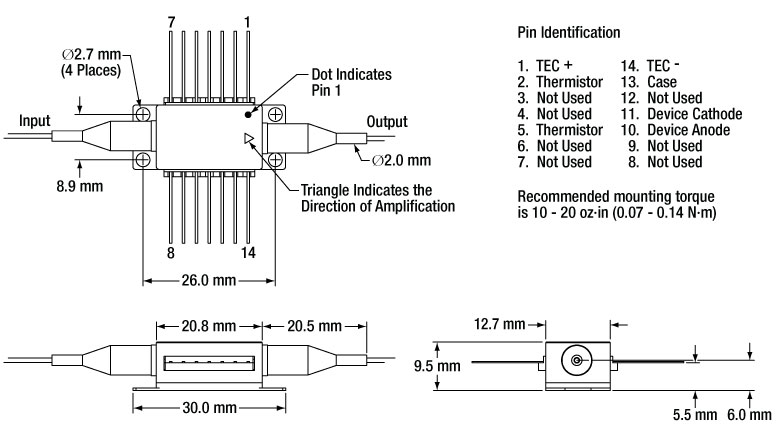
ピン配置図と図面
注:すべてのグラフは典型的な性能を示しており、ユニットにより「仕様」タブ内の仕様値の範囲内で若干異なる可能性があります。
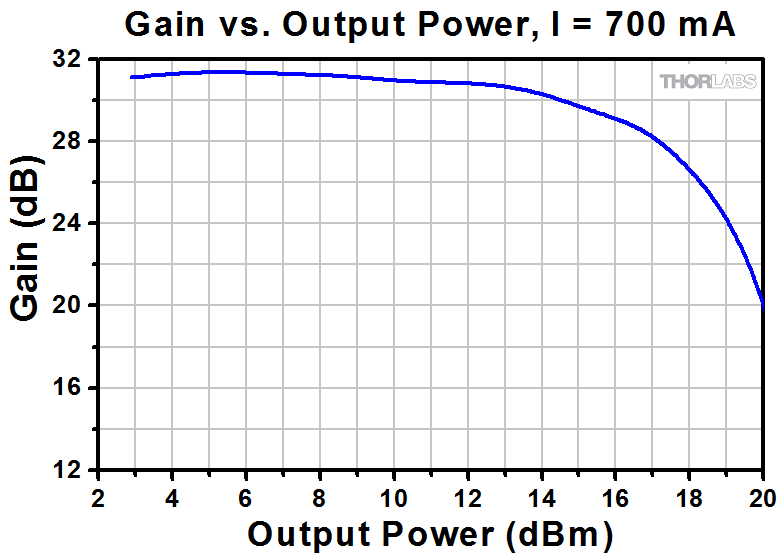
BOA1130S&BOA1130Pのグラフ
BOA1130SおよびBOA1130PのGain vs. Output Power(利得と出力の)曲線は、駆動電流700 mA、入射波長1312 nmで測定されたものです。ASEスペクトルも駆動電流700 mAで測定されています。


BOA1310S&BOA1310Pのグラフ
BOA1310PのGain vs. Output Power(利得と出力の)曲線は、駆動電流900 mA、入射波長1312 nmで測定されたものです。ASEスペクトルも駆動電流900 mAで測定されています。BOA1310Sは同様の性能を示します(詳細については下記型番横の赤いアイコンをクリックしてSpec Sheetをご覧ください)。


BOA1132S&BOA1132Pのグラフ
BOA1132SとBOA1132PのGain vs. Output Power(利得と出力の)曲線は、駆動電流700 mA、入射波長1312 nmで測定されたものです。ASEスペクトルも駆動電流700 mAで測定されています。

BOA1017P&BOA1017Sのグラフ
BOA1017PおよびBOA1017SのGain vs. Output Power(利得と出力の)曲線は、駆動電流600 mA、入射波長1312 nmで測定されたものです。ASEスペクトルも駆動電流600 mAで測定されています。


BOA1036P&BOA1036Sのグラフ
BOA1036PとBOA1036SのGain vs. Output Power(利得と出力の)曲線は、駆動電流700 mA、入射波長1312 nmで測定されたものです。
ASEスペクトルも駆動電流700 mAで測定されています。注:下のASEスペクトル曲線のリップルは、試験中の水の吸収に起因するものです。
デバイスの性能を示すものではありませんのでご注意ください。


半導体光増幅器(BOAおよびSOA)は、シングルパスの進行波増幅器で、単色信号あるいは多波長信号の両方において性能を発揮します。偏光依存型半導体光増幅器(BOA)は1つの偏光状態のみを増幅するので、入力光の偏光状態が分かっている条件での使用に適しています。これに対して入力信号の偏光状態が不明の場合や変動する用途では、偏光無依存型半導体光増幅器(SOA)が必要となります。しかしながら利得、雑音、バンド幅や飽和出力強度の仕様は、偏光依存型(BOA)の方が偏光無依存型(SOA)と比較して優れています。これは偏光無依存型(SOA)では偏光無依存の特性を付与している設計により上記特性が犠牲になっているためです。
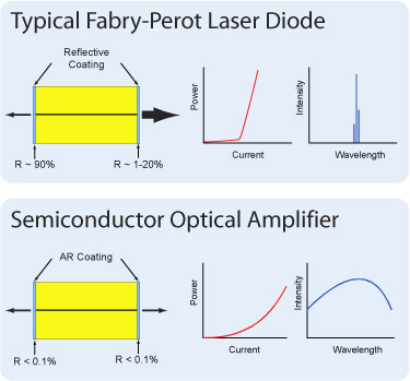
半導体光増幅器はファブリペローレーザと似た設計ですが、相違しているのは、ファブリペローレーザでは、半導体チップの両端面に反射コーティングが施されている点です。両端の反射面からの戻り光が共振器として機能し、レーザ発振が生じます。半導体光増幅器では、半導体チップの両端面に反射防止(AR)コーティングが施されています。これによりチップに戻る光は制限されるので、レーザ発振は生じません。
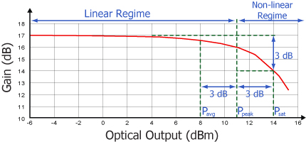
全ての増幅器に共通する典型的な特性ですが、半導体光増幅器にも2つの動作領域があります。1つは線形でフラットな一定利得の領域で、もう1つは非線形で出力が飽和する領域です。変調信号を増幅するのに使用されるのは一般に線形領域で、そこではパターン効果、マルチチャンネルクロストーク、エルビウムドープファイバ増幅器(EDFA)でも見られる過度応答といった問題が発生しません。非線形領域は、半導体利得媒質の高非線形性(相互利得変調や相互位相変調)を活かして、波長変換、光3R再生、ヘッダ認識、その他の高速光信号処理などに利用されます。
CW入力信号では、増幅器が生成できるパワーの合計は飽和出力(Psat)のパラメータで決定されます。Psatは、小信号利得が3 dB低くなる出力で定義されます。一般的に出力可能な最大のCWパワーは、飽和出力よりもおよそ3 dB高くなります。
| Posted Comments: | |
Guilherme Garcia
(posted 2022-03-23 10:24:54.263) I am using a BOA1130P - Booster Optical Amplifier.
I would like to have a better understanding for the behavior of this component, and was wondering if you could give me directions about the original work published on this area?
Like papers published on specialized journals or conferences.
Thank you very much
Guilherme jdelia
(posted 2022-03-24 01:51:08.0) Thank you for contacting Thorlabs. I have contacted you directly to recommend some literature for this subject area. Generally, Booster Optical Amplifiers (BOA's) and Semiconductor Optical Amplifiers (SOA'S) are the same, Thorlabs uses the term "BOA" to describe a special case of a SOA that is polarization dependent. Kenny Wong
(posted 2020-04-10 02:01:36.62) I am looking for a component to amplify the output from my tunable laser (Santec TSL 550) from around 12dBm to above 16dBm. Can your BOA do the job? YLohia
(posted 2020-04-23 12:43:45.0) Thank you for contacting Thorlabs. What specific wavelength range do you plan on using from your laser for amplification? Are you planning on continuously sweeping through the wavelengths? Or are you planning on discretely stepping through the wavelengths over a long period of time? I had contacted you at the time of your original post with these questions and did not receive a response. If you would like to continue this discussion, please email us at techsupport@thorlabs.com. Luluzi Lu
(posted 2019-11-05 14:14:29.587) How about the polarization dependent gain? And do u sell the o-band SOA chip? YLohia
(posted 2019-11-12 12:26:37.0) Hello, thank you for contacting Thorlabs. What specific BOA are you asking for the PDG of? Unfortunately, we currently do not offer polarization insensitive SOAs in the O-band. Chih Liu
(posted 2019-03-25 16:05:37.4) Dear Sir,
Could you please let me know the spontaneous emission power of the BOA1017S? We are planing to build an system by using this amplifier.
Thank you
Chih YLohia
(posted 2019-03-28 05:03:49.0) Hello Chih, thank you for contacting Thorlabs. I have reached out to you directly with a plot of the total ASE power vs drive current. kkmion
(posted 2018-11-28 22:31:19.793) Can the BOA be driven using CLD1015? YLohia
(posted 2018-11-29 08:50:59.0) Yes, the BOA can be driven using the CLD1015. This information is given on the Overview tab of this page. jeffrey.o.white6.civ
(posted 2016-05-02 09:02:18.21) I would like to know how much spontaneous emission comes out when, for example, 4mW is input, and 40mW (or max output) is produced. Do you have any output spectra representative of these devices for a seed in the O-band. Thx.
Jeff White besembeson
(posted 2016-05-04 02:53:59.0) Response from Bweh at Thorlabs USA: For a 700mA drive current, we have a plot for the amplified spontaneous emission spectrum (ASE) under the "Graphs" tab. The gain variation with output power was measured at 1312nm, which is in the O-band. udaytronic
(posted 2016-04-26 07:28:56.21) Hi,
I was looking for maximum input optical power for those amplifiers in the specs. But I don't see them. Could you please let me know where to find or may be you can update them.
Thanking you besembeson
(posted 2016-04-26 09:46:56.0) Response from Bweh at Thorlabs USA: We do specify the saturation power, and the maximum output power that can be extracted from any of these devices is 3dB higher than the saturation power. So you should keep your input power to a maximum level with the amplification factor (which is wavelength and drive current dependent) and saturation power in mind. |