 Products Home
単結晶ダイヤモンド
- Diamonds Grown by Chemical Vapor Deposition
- Quantum-Grade or Electronic-Grade Diamonds Available
- Uniform Distribution of NV Centers
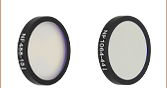
ELSC45
NV: <0.03 ppb
4.5 mm x 4.5 mm x 0.5 mm
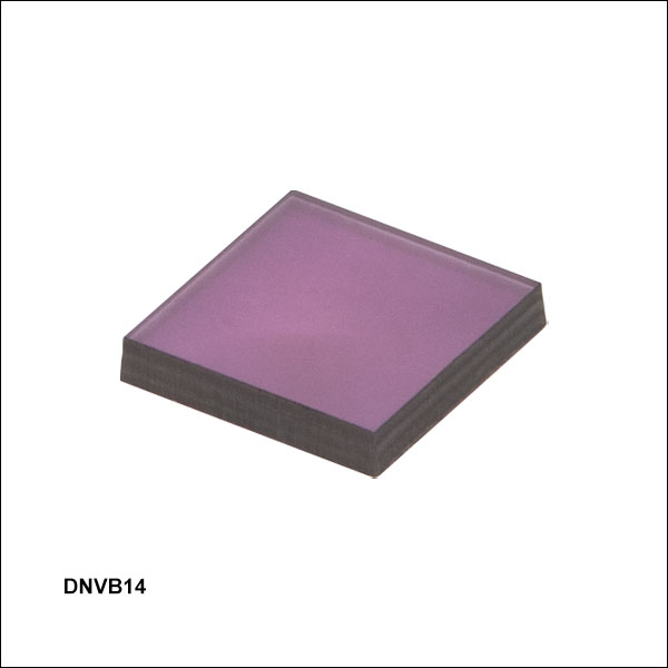
DNVB14
NV: 4.5 ppm
Coherence Time T2: 10 µs
3.0 mm x 3.0 mm x 0.5 mm
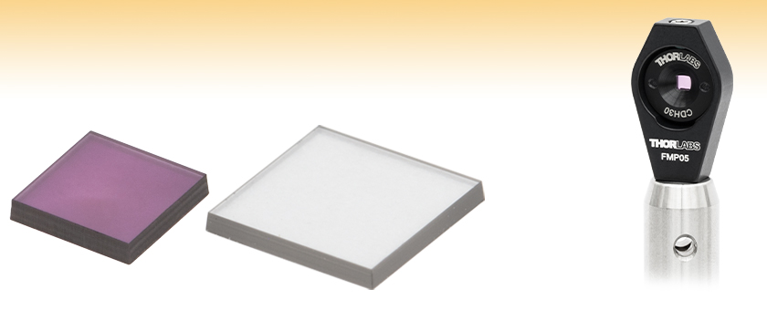
Application Idea
A DNVB14 3.0 mm square quantum-grade single-crystal diamond is mounted in an FMP05 Ø1/2" optics mount using a CDH30 square optics holder.


Please Wait
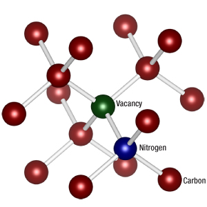
NV中心は、窒素原子と隣接する空孔が、
ダイヤモンド格子の炭素原子のペアに置き換わる点欠陥です。
特長
- 化学気相成長法(CVD)により生成された単結晶ダイヤモンド
- 量子グレードまたは電子グレードのダイヤモンドをご用意
- 窒素-空孔中心(NV中心)中心の濃度: 0.03 ppb以下、300 ppb、4.5 ppm
こちらの単結晶ダイヤモンドは、Element Six社が特許を取得したプロセスによって製造し、量子研究の発展のために当社から提供されている製品です。磁場センシング、RF検出、ジャイロスコープ、メーザ、量子技術のデモンストレーション、量子計算、量子通信、および研究用途に適しています。量子グレードのダイヤモンドは、窒素-空孔中心(NV中心)の濃度300 ppbまたは4.5 ppmでご用意しております。欠陥中心をご自身で作成されたい場合は、NV濃度が0.03 ppb以下で、バックグラウンド不純物が少ない電子グレードのダイヤモンドもございます。これらのダイヤモンドは耐電離放射線性のデバイス製造などの用途にご使用いただけます。
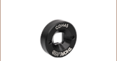
当社のオプトメカニクス部品に単結晶ダイヤモンドを取り付けるには、マウント無し正方形光学素子用のØ12.7 mm(Ø1/2インチ)アダプタのご使用をお勧めいたします。

Click to Enlarge
ゼロ磁場でのダイヤモンドNV–中心のエネルギーレベルの概略図。スピンの三重項基底状態(3A2)と励起状態 (3E)との間のエネルギー差は637 nm (1.945 eV)で、それぞれが一重項に縮退するms = 0 および二重項に縮退するms = ±1のスピン状態に分裂し、エネルギーの差はそれぞれDgs = 2.88 GHz (12 µeV) と Des = 1.42 GHz (5.9 µeV)になります。なお、ここではスピンのサブレベルの分裂が視認できるよう大幅に誇張されています。また、光強度が弱い2つの中間状態ms = 0 (1A と 1E)のもあり、このエネルギー差は1042 nm(1.190 eV)です。

Click to Enlarge
The NV-中心の三重項基底状態は、スピン-スピンの相互作用により、ms = 0 と ms = ±1の間で構造分裂(Dgs = 2.88 GHz)を示します。[111]の欠陥の軸に沿って外部磁場(B)を印加すると、ms = ±1状態がゼーマン効果によりさらに分裂(ΔE = 2gµBB)します。ここでg はランデの因子、µBはボーア磁子です。

| Posted Comments: | |
Jano Gil Lopez
(posted 2025-01-17 10:51:36.037) Dear Thorlabs team,
We would like to know if it is possible to experiment and test quantum memories with these products. We would need low density NV centers. Do you have any customers who have succesfully used them? Thank you.
Best regards,
Jano tdevkota
(posted 2025-01-21 04:52:07.0) Thank you for contacting Thorlabs. In principle, these materials can be used as a key element in a quantum memory setup. I have reached out to you directly to discuss your application further. Marcel van der Horst
(posted 2024-06-13 09:35:21.457) Dear sir, madam,
At the Amsterdam University of Applied Sciences, we want to develope our own NV-center magnetometers.
Can you please inform me how many diamonds are delivered when I buy "quantity 1" DNV B14 diamonds; is it one diamond or several diamonds in a package?
Thank you in advance for the information.
Best regards,
Dr. Marcel van der Horst
Amsterdam University of Applied Sciences/Sensor lab
Jakoba Mulderhuis, Rhijnspoorplein 2, 1091 GC Amsterdam
M: 06 2115 8862
http://www.hva.nl/opleiding/engineering-elektrotechniek/elektrotechniek.html?origin=euCvyOz3R2q5%2B5c%2BeyU0bQ jdelia
(posted 2024-06-13 12:34:04.0) Thank you for contacting Thorlabs. The DNVB14 consists of one diamond doped with NV-centers. Hassan TERMOS
(posted 2024-03-20 10:26:40.817) Dear Sir,
I would like to ask you if this type of crystal has fixed or variable grating periods.
The threshold power and maximum input power can depend on various factors, including crystal quality, pump wavelength, pump intensity, temperature control, and phase matching conditions. I already used a PPLN crystal; the threshold power was 4-6 W, while the maximum input pump power that crystal can afford is 20 W. The pump wavelength of the PS laser is 1064 nm.
Can I know the threshold power that indicates the minimum power required for efficient parametric generation to occur in the crystal and the maximum input pump power that represents the upper limit?
Best regards,
Hassan Termos jdelia
(posted 2024-04-04 12:55:25.0) Thank you for contacting Thorlabs. While PPPL has a periodicity associated with it, it does not really apply to diamond. Diamond is also not a traditional non-linear crystal so we can’t really suggest anything about pump lasers required. I have reached out to you directly to clarify your inquiry and discuss your application further. Benjamin Strycker
(posted 2023-10-04 16:18:30.397) For the NV diamond products, are the NV-axes oriented preferentially along the {111} direction, or are the NV-axes randomly oriented along the four crystallographic directions allowed in diamond? cdolbashian
(posted 2023-11-08 01:04:46.0) Thank you for reaching out to us with this inquiry. NVs will be randomly distributed amongst the four possible <111> directions with no preferred direction. Jing Zhou
(posted 2022-09-02 21:37:48.633) 您好,我想问一下关于:
1.DNVB1参数表里的Edge Features是什么意思?
2.NV色心在金刚石晶片表面均匀分布吗?
3.晶片中制作好的NV色心的深度(与上表面的距离)是多少? |

 ズーム
ズーム| Item # | DNVB1 | DNVB14 | |
|---|---|---|---|
| Quantum Properties | |||
| Typical NV Center Density | 300 ppb | 4.5 ppm | |
| Typical Spin Coherence Time T2* a | 1 µs | 0.5 µs | |
| Typical Spin Coherence Time T2 b | 200 µs | 10 µs | |
| General Specifications | |||
| Crystallographic (Face) Orientation | {100} ± 3° | ||
| Edge Orientation | < 100 > | ||
| Dimensionsc | Length | 3.0 +0.2/-0.0 mm | |
| Width | 3.0 +0.2/-0.0 mm | ||
| Thickness | 0.5 ± 0.05 mm | ||
| Laser Kerf | ≤ 5° | ||
| Edge Features | < 0.2 mm | ||
| Roughness, Ra | < 10 nm | ||
| 13C Fraction | 1.1% | ||
- NV中心の濃度は2種類ご用意
- DNVB1: 300 ppb
- DNVB14: 4.5 ppm
- サイズ: 3.0 mm x 3.0 mm角
量子グレードのダイヤモンドは、窒素-空孔中心(NV中心)の濃度300 ppbまたは4.5 ppmでご用意しております。これにより、読み出しや書き込みが可能なスピン量子ビットを伴ったNV中心が作られます。 このスピン量子ビットは室温でも長寿命であり、 ダイヤモンドの構造や強い共有結合に起因する利点も有しています。こちらのダイヤモンドは、NVスピン中心の濃度、均一な分布、スピン特性、コンパクトな形状因子により、磁場センシング、RF検出、ジャイロスコープ、メーザ、量子技術のデモンストレーションや研究用途に適しています。ダイヤモンドは3.0 mm x 3.0 mmでご用意しており、当社のマウント無し正方形光学素子用のアダプタCDH30に取り付け可能です。
なお、損傷を避けるため、これらのダイヤモンドは先端がカーボンファイバのピンセットTZ1のような非金属の工具で取り扱う必要があります。

 ズーム
ズーム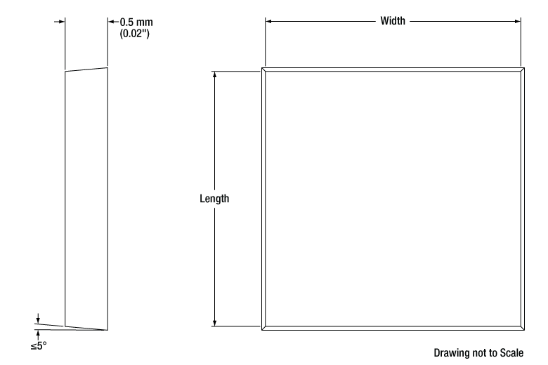
| Item # | ELSC20 | ELSC40 | ELSC45 | |
|---|---|---|---|---|
| Crystallographic (Face) Orientation | {100} ± 3° | |||
| Edge Orientation | <110> | |||
| Dimensionsa | Length | 2.0 +0.2/-0.0 mm | 4.0 +0.2/-0.0 mm | 4.5 +0.2/-0.0 mm |
| Width | 2.0 +0.2/-0.0 mm | 4.0 +0.2/-0.0 mm | 4.5 +0.2/-0.0 mm | |
| Thickness | 0.5 ± 0.05 mm | |||
| Laser Kerf | < 5° | |||
| Edge Features | < 0.2 mm | |||
| Roughness, Ra | < 5 nm | |||
| Boron Concentration | < 1 ppb | |||
| Nitrogen Concentration | < 5 ppb | |||
| Typical NV Concentration | < 0.03 ppb | |||
| 13C Fraction | 1.1% | |||
- 低い窒素-空孔中心(NV中心)濃度: 0.03 ppb以下
- 3種類のサイズをご用意
- 2.0 mm x 2.0 mm角
- 4.0 mm x 4.0 mm角
- 4.5 mm x 4.5 mm角
こちらの電子グレードの単結晶ダイヤモンドは、5 ppb以下の窒素濃度と、通常0.03 ppb以下の窒素-空孔中心(NV中心)濃度を有します。また、バックグラウンド不純物がホウ素濃度1 ppb以下と非常に低く、通常2000 cm2/V⋅sを超える電子移動となります。これらのダイヤモンドを使用して、as-grownのNV欠陥を調べたり、イオン注入またはエピタキシャル成長によって独自のNV欠陥を生成したりすることができます。また、放射線検出器などのカスタム仕様のダイヤモンド電子デバイス用だけでなく、高出力レーザやマイクロ電子デバイス用に、高い熱伝導性および光学的な透明性を有するヒートシンクとして利用する用途にもお使いいただけます。ダイヤモンドのサイズは2.0 mm x 2.0 mm角、4.0 mm x 4.0 mm角、4.5 mm x 4.5 mm角でご用意しており、また当社のマウント無し正方形光学素子用Ø12.7 mm(Ø1/2インチ)アダプタに取り付けが可能です。
なお、損傷を避けるため、これらのダイヤモンドは先端がカーボンファイバのピンセットTZ1のような非金属の工具で取り扱う必要がありますのでご注意ください。